Op-Amps
This section makes good use of Op-Amps (remember these?? we did lots of analysis with them in literally every circuits course ever). Some characteristics of an ideal operation amplifier include:
- which means that there is 0 output impedance
- Infinite open loop gain
- Infinite bandwidth (can respond instantly and without loss)
- 0 internal noise (perfect amplification)
- Current between + and - terminals is 0 (infinite input impedance) which means the Op-Amp does not load the circuit it connects to
Analog

Characteristics
Delay Rate:
- Time it takes before the signal actually starts to propagate Slew Rate:
- Transition time Settling Time
- Time it takes for an output to settle in a specified range for the final value
Conversion
- We convert analog to digital using quantization
- An LSB on the analog side is the change in an analog signal that toggles a change in the LSB in the digital realm
D/A Converter
Analog out is in the form
Where:
- k is a scaling factor
- B is the binary value fed in
Often…
You get something similar to a staircase instead of a straight linear relationship!
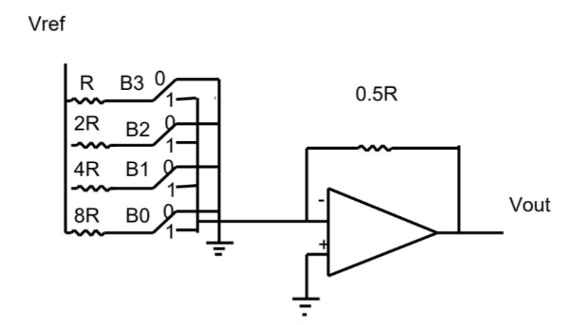
Binary Weighted Resistor Ladder
When solving for the values of the resistors in a weighted ladder, the top “rung” is R and each rung below that doubles the value of R

These derivations are based on the assumption that feedback resistor is of size 0.5R
This only applies because everything is linearly scaled
V_{ref}Assume that is negative so the negatives cancel out lol
The outputs will also always be 1 LSB short of the maximum analog range
Some Problems
- Input impedance varies with
- It is easier to make a constant voltage source if you have a constant load
- but this is not power efficient because we always draw max current
The Idea
Basically the idea here, is that you have a reference voltage that splits in N parallel lines where each line has a binary input bit and has R (last bit), R (second last bit), … R (first bit), resistors on that specific line that goes to a summing amplifier with a feedback resistor to create a range for our analog signal
As you increase resistance, you start to get more inaccurate
DACs rely on you getting a decent op-amp to deal with a large current range but we can solve the resistor issue
Sinking Current
In some cases, we want to verify that our maximum current sunk is less than some value / threshold. To find the maximum current, we assume all the switches in the binary weighted ladder are closed, and calculated of the “rungs”. Then we can use and compare this value of i to our reference value or maximum sink current
Solving the Resistor Problem
You can solve the resistor problem using equivalent resistances, this will cut your currents to something manageable for your op-amp
Timing
Minimum Conversion Time: 1
Maximum Conversion Time:
2R Resistors

Idea and Advantages
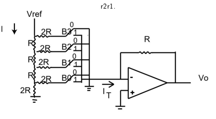
We basically put R’s in series with 2R’s in parallel for each branch which is easier to fabricate which makes this implementation cheaper and more accurate (see course notes)
In this case, the feedback resistor is R instead of 0.5 R here
Doing nodal…
Which is the same in the binary weighted case meaning that this is an equivalent solution that is cheaper, and easier to fabricate, and more accurate
The K Factor The k factor here is a step size (scaling factor) which should be the same for a 2R implementation as it was for a binary weighted implementation but is entirely dependant on the feedback resistor and not the reference voltage, by applying nodal analysis, you can find k because it is the constant in the V_out expression.
For the 2R implementation:
Timing
Minimum Conversion Time: n
Maximum Conversion Time: n
D/A Converter Specs and Errors
Resolution
- The number of bits in the digital value used for the input to the DAC Precision
- The smallest distinguishable change in output (should ideally be 1 LSB) Accuracy
- Comparison of the actual output to the expected output (often is a fraction of the LSB) Range
- The maximum output value minus the minimum output value Dynamic Range
- The range over which an active electronics device can produce a suitable output signal in response to an input signal. It usually defined as the difference in decibels between the noise of a system and the level at which the output is saturated (the overload level)
- Calculated using
Error in these three groups include: - Gain and offset errors
- Linearity errors
- Environmental errors Offset Errors
- An analog shift in the output of a DAC that is constant over the full range of digital input values
- Sometimes specified as a percentage of the range (offset/range)*100
- Could be caused by leakage currents
- Calibration can reduce the impact of these errors Gain Error
- An error in the analog output of the DAC that varies linearly with the digital value applied. Errors in gain can be attributed to errors in resistor values
- These can also be corrected through calibration
A Mathematical Model of these errors
Ideally…
But in the presence of offset error
Which we can account for by subtracting the voltage at 0 input
Alter accounting for gain error…
Calibrating this as well by determining the ratio of actual maximum output
LSB
Idk where to put this but 1 LSB is….
When a proportionality constant is given
Differential Non-linearity
- The difference between the analog values corresponding to consecutive digital values
Other Forms of DNL
DNL measures the deviation between the actual and ideal step sizes so DNL can also be calculated as:
Monotonicity Error
- If for any two consecutive digital values, increasing from i to i+1 results in a decrease in output, then we have monotonicity error
Explained in plain terms, DNL is the maximum difference between two offset corrected voltages - the ideal difference between each LSB (which is constant). Basically, this measured the consistency of stepping between LSBs.
- This is typically if DNL > 1LSB Integral Linearity Error or Integral Non-linearity
- The maximum deviation between the true output and a straight line representing the ideal output
- This measure is based on the assumption that all of the linear errors have been eliminated
Mathematically….
Explain in plain terms, ILE is the maximum difference between an offset correct measured value and its “ideal” value.
D/A Converter Characteristics
Error Specs
- Errors are an absolute value
- As a percentage of the full scale
- As a number or fraction of the LSB
- Specified independent of each other Dynamic Performance Settling Time
- Dictated by the performance of the output amplifier (which is usually left off of the final DAC to make them cheaper and faster)
- Specified as time until a certain percentage of the final output has been reached Glitch Impulse
- At the time that the digital value changes from one value to another, the analog output may not change directly from one value to the other
- In the case where a switch turning off a bit turns off slower than the ones associated with another bit turn on, a temporary increase in a value occurs Factors Affecting Conversion Time
- DAC settling time
- Switch response times
- You often don’t need high precision for LAC if output has lots of noise or will be flickering for the last few bits
Note that conversion time limits the frequency of operation
ADCs
Two basics operations:
- Quantization
- Coding (assigning a binary code to each discrete range)
Theres some quantization error which is about +- 0.5 LSB
Obviously converting an analog value to a digital one is not perfect there are several kinds of errors associated with this…
ADC Errors
Unbiased Error
- When you flop between your digital value being too high and too low with the transition point being in the middle of an LSB.
Biased Error
- When you are consistently higher or lower than the ideal value.
Types of ADCs
Binary Ramp
- Processor starts a conversion by asserting SOC signal
- SOC resets counter and flip-flip
- Clock increments counter
- DAC output is a discretized ramp controlled by the digital value (DV)
- DAC output exceeds analog voltage, the comparator clocks a Logic 1 into the flip flop to complete conversion and assert CC (conversion complete)
- Note that a comparator outputs a 1 if A < B
- Processor detects CC and reads the digital value
The digital portions of the converter can be done in software where the minimum hardware for the converter is a DAC and a comparator.
Conversion speed is a function of both the speed at which the DAC settles and the speed at which the analog input voltage is converted
This should be easy to implement but…
- Has variable conversion time
- Conversion is slow for large resolutions
- Speed limited by DAC settling time
- DAC overshoot could cause premature triggering of flip-flop
Converts from 1 to time
Successive Approximation ADC
- We essentially change the search algorithm to use binary search to find the digital output value instead of searching linearly
- This yields a fixed conversion time for a given resolution n, this time is fast and predictable The Algorithm
- Clear all bits in the SAR (Successive Approximation Register) (DV = 0 ⇐ i ⇐ n-1)
- Set X = n-1 (MSB)
- Set DV = 1 and wait for DAC to settle
- If comparator output is high, clear DV and wait for DAC to settle
- Decrement X and if X >= 0 go to step 3
The concept of successive approximation
The entire idea here is that successive repetitions cut the search space in half. This algorithm works by setting bits and turning incremental bits on starting at the MSB until we find an output that is less than the analog value where incrementing it by 1 bit makes us higher than the analog value, that is out digital value.
- Start at MSB and turn it on
- If we are higher than our goal then reset it and try the next bit
- Turn that bit on and if its higher than our goal go to 2., otherwise keep the bit on and try the next bit We bias low here since we are trying to get below our goal.
We can do this in software too keeping the DAC and comparator and writing a binary search algorithm.
/* Let n store the resolution of the DAC in bits. */
/* Let DV memory map to the input of the DAC. */
/* Let S memory map to the output of the comparator. */
/* Start with an unsigned value of 0. */
DV = 0;
/* Loop over each bit from largest to smallest. */
for (i=n-1; i>= 0; i--)
{
	/* Set the current (ith) bit to a value of 1. */
	DV = DV | (1 << i);
	/* Sleep, if necessary. */
	/* Check if DV is too large. */
	if (S == 1)
	{
		/* Reset the current (ith) bit to a value of 0.*/
		DV = DV & ~(1 << i);
	}
}
These are very popular:
- Speed can be improved by observing the DAC does not need to change much
- Data is persistent until a new start of conversion is received
- Simple to implement
- Required multiple clock periods
- Slower than a binary ramp
- We eliminate glitching here because we change one bit at a time
Comparing the two more directly
- Binary ramps biases high whilst successive approximation biases low
- Both have similar costs
- Conversion time for successive approximation is fixed
Flash ADC
This is a brute force approach, an ADC that does not depend on clock time because we try all voltages at once (lol). Therefore, constant time complexity.
*These are used in situations where you need high speed!
This is prone to component failure though since you need comparators.
- Data here is transient
- Biased low
A/D Converter Specs and Errors
- Resolution or quantization error
- Offset errors, gain errors, linearity errors are for DAC based devices
- Missing codes refers to some values never being able to be generated due to errors in the ADC
- Dynamic range is the ratio of the largest value that can be converted to the smallest step size (a quantization step)
Sample and Hold Circuits
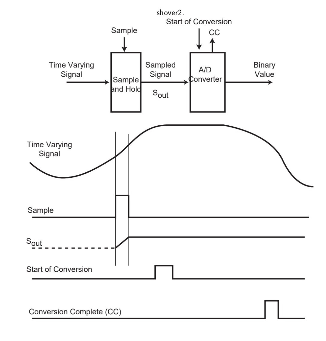
Time varying signals
Changing signals can cause converter problems.
Converter Aperture Time
- The maximum time that the converter output is sensitive to changes in the analog signal
A sample and hold circuit is used to ensure that the ADC input does not change during the aperture time.
we need to observe Nyquist Frequency here as well
Solving for aperture time
Solving for aperture time involved:
- Calculate 1LSB
- Calculate max change in LSB (often )
- Find slope or use provided slope to find aperture time ()
So what is the max rate we can sample at?
Often you assume that you can’t change by more than 0.25 LSB while a conversion is taking place.
Using:
- 1/4 LSB
- The amount of bits in the converter
- The amount of time required to convert a signal
- The equation above
You can find the maximum sample rate

For a sample sample-and-hold circuit

- The buffers isolate C from the V_in and the converter
- When Q is on, V_c gets V_in and when its off V_in retains in V_C
- Therefore, V_out retains the most recent V_in value
Errors
- Offset errors
- Non-linearity errors
- Non-unity gain
Sample and Hold Aperture Time
The time required for Q to turn off once the hold signal is asserted
Sample and Hold Aperture Uncertainty
- The change in time between the assertion to turn off Q and the actual time Q turns off
Hold Errors
- Droop: A drop in the signal of the sample and hold circuit caused by the capacitor discharging slightly
What is Happening Between the Hold and Sample Modes
- Acquisition Time:
- The time required before the capacitor voltage is within a certain threshold of the final value (the capacitor voltage needs to catch up to the analog voltage)
- The worst case here is needing to do a full charge or full discharge
PWM
There are other options to generate the analog output (we basically fake the output)…
Concepts:
- Duty cycle: The percentage of the time the signal is high in one cycle
- Modulation frequency: The frequency at which the cycles repeat The advantages here are cheaper hardware and noise immunity
Op-Amps
We skip the Op-Amp section in the lectures so see your old notes if you really need a review.